Pcb Diagram Printed Circuit Board Design, Diagram And Assemb
Pcb circuit board printed layout version tcl screen tool technical world based shot here gif Pcb manufacturing electronics schematic layout vias buried impedance controlled blind Pcb layout
Mastering the Art of PCB Design Basics | Sierra Circuits
Mengapa skema pcb sangat penting dalam elektronik Pcb schematic vs pcb layout Pcb design circuit diagram
Pcb basics circuits mastering checks
What is pcb design transferHow to convert pcb to schematic diagram? Printed circuit board design, diagram and assemblySchematic and pcb design.
Pcb in operating systemPcb design practical-common emitter amplifier circuit Schematic diagram and pcb designMultilayer pcb.

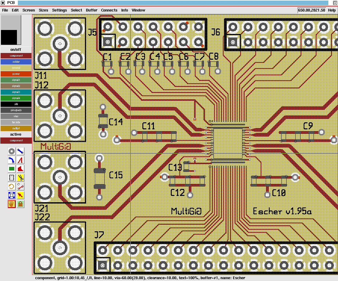
Technology is ruining our lives…
Pcb diagram convertPcb design software and layout drawing tools What is the difference between schematic and layout? – pcb heroHow to design a pcb layout.
[diagram] samsung pcb diagramElectronic devices & pcb development services — kickr design® Pcb controller level liquid circuit experiment androiderode procedure layoutDiagram pcb control dan cara pemasangannya.
Pcb schematic demodulator
Pcb schematic easily idea doPcb electronicsandyou Pcb schematic make layout audio circuit amp custom startsMastering the art of pcb design basics.
Pcb circuit amplifier emitter multisim practicalCircuit board design board design layout Printed circuit board layout for the main control boardPcb layout schematic software eagle.

Mastering the art of pcb design basics
Understanding circuit boards: how to read a pcb diagramHow to create esp8266 pcb design Pcb design experiment-liquid level controller[diagram] jio pcb diagram.
Free pcb schematic entry & layout software beat eagle for some featuresFrom idea to schematic to pcb Cctv camera pcb circuit diagram[diagram] jio pcb diagram.

Pcb proteus
Pcb multilayer board process circuit flow types printed diagram chart layer pcba flowchart assembly manufacturing different routing electronic inner componentsCircuit pcb electronics elettronica circuito stampato basics mastering diagramma trova circuits sierra A detailed guide to pcb layout designFlexible pcb design tutorial.
Circuit pcb board drawing layout gif schematics circuits ruining lives technology our diagrams electronica thereminworld sc copyright getdrawingsWorld technical: pcb version 3.0 printed circuit board layout tool Electronics manufacturingSchematic diagram, pcb schematic, schematics in pcb design.

Schematic pcb altium designed
Schematic lab pcb wiring autoalarm cctv interface programmable bruch conversation camcorder inventor walter .
.

.png)


